Photovoltaics

In recent decades the energy issue has become a common discussion topic. We may eventually deplete the fossil fuels that can be economically extracted.[1] Depletion is not the only issue involved in the use of fossil fuels; the combustion process releases carbon dioxide which can alter climate. Fossil fuels, such as coal, natural gas, and oil, are the most common energy sources used today. When combusted to create energy, these fuels release carbon dioxide, a greenhouse gas. These emissions can cause a warming effect on the planet. The exact results of this warming are not certain, since recent trends as of 2021 show increases in Arctic sea ice and other cooling data.
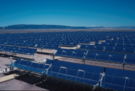
One promising renewable energy source involves capturing the energy of the sun through photovoltaic technology; this a process is like the most common means of collection and utilizing solar energy; however, one problem is that solar panel manufacture is a chief source of Nitrogen Trifluoride, a much more powerful and long lasting greenhouse gas compared to carbon dioxide. Other adverse issues of solar panels are the use of large amounts of toxic heavy metals such as arsenic and cadmium. Further adverse impacts of large solar arrays are habitat destruction of deserts and other ecosystems.
Contents
Solar radiation
The sun is a giant ball of mostly hydrogen that is constantly undergoing fusion nuclear reactions to form helium and in the process releasing a huge amount of radiation energy. Some of that energy is released in the form of photons. The sun is estimated to produce approximately 100 billion billion Megawatts (MW) of power, but only a small fraction (200 billion MW) reaches the earth.[2] The sun’s radiation is the basic energy source for the plant, providing heat, allowing plants to grow, driving weather patterns, and providing other vital services. Solar radiation can also be harnessed and converted to electricity for human use by photovoltaic solar cells, the details of which will be explained below.
Production and materials
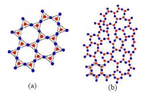
Solar modules used to harness energy from the sun are made up of photovoltaic cells much the way human tissue consists of cells. Photovoltaic cells are constructed of semiconducting materials, usually silicon. The cells use either crystalline silicon or amorphous silicon. All crystalline solids have a high molecular order at all levels, meaning their atoms are placed at very regular intervals.[3] Amorphous solids have a similar molecular order to crystals at a small scale because they have the same number of atoms in their lattice, but amorphous solids have less order than crystals at a larger scale because the distances between the atoms are not all equal, as seen here to the right. These differences result because amorphous solids solidify at a lower temperature and in less time than crystals.

How they work
Semiconductors allow current to flow through them, but are orders of magnitude less conducting than conductors.[4] Pure silicon acts as an insulator, but by doping the silicon with phosphorus, an element with five valence electrons, an n-type semiconductor is created.[5] Valence electrons are farthest from the nucleus of the atom. Because silicon has four valence electrons, phosphorous provides additional electrons to the silicon crystal lattice so that there are more electrons in an n-type semiconductor than there are places for them to fit into the lattice.[6] These extra electrons will carry electric current and thus are called the majority carriers of n-type semiconductors.

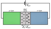
Semiconductors can also be of p-type. Dope silicon with boron, which has three valence electrons, to create a p-type semiconductor. P-type semiconductors have “holes,” which are empty places for electrons in the lattice, as their majority carrier because boron has one less valence electron than silicon. When the two types of semiconductors are placed next to one another they form a p-n junction where holes drift from the p-side to the n-side and free electrons drift in the other direction. This movement of charge (negative electrons) produces an electrical field across the junction, or the location where the two sides meet. Negative ions are left behind when a hole leaves the p-side and positive ions are left behind when a free electron leaves the n-side. These create a dipole layer at the junction that produces an electric field that opposes more majority carriers traveling to the opposite side of the p-n junction. This electric field will aid in the generation of electricity, as will be explained in further sections.
Single crystalline solar cells
[[Image:li-9802.fig.7.lg.gif|frame|left|http://www.tms.org/pubs/journals/JOM/9802/Li/Li-9802.html </font></span> </span>
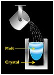
The two main kinds of solar panels, single crystalline and multi-crystalline, on the market today are made from silicon. The original production method of photovoltaic cells produces a single-crystalline cell by growing a column from a single seed crystal of high grade silicon using the Czochralski method.[7] In the Czochralski method the seed crystal is lowered into a crucible of molten silicon and pulled out slowly while rotating constantly so that the crystal forms a column.[8] A wafer cut from the crystal column becomes a solar cell.
These cells are only a few square inches in area so several are connected and placed on a backing material to be sold as a module (also called a solar panel).[9] Cells produced with the Czochralski method are circular, so edges are trimmed to fit better on a module, but because they cannot cover the entire area completely they lose efficiency per unit area. The crystal wafer is doped with boron to make a p-type semiconductor. It then goes through a series of polishing and etching processes so that it will absorb a higher percentage of solar radiation. Phosphorous is then diffused onto one side to create an n-type semiconductor layer and a p-n junction where the two semiconducting surfaces meet. The cell now has a p-n junction, but can only generate an electrical current if it is connected to a circuit.

The cell is connected to a circuit by inserting conductor contacts onto each side of the cell, starting with the n-side. These contacts are usually made from a silver paste applied in a grid formation or are screen-printed to the surface. After the contact is attached, an anti-reflection coating, usually titanium dioxide, is added to the n-surface of the cell. Next the contact is formed on the p-side by annealing an aluminum layer to p-side. With all the contacts in place, the cell is ready to be connected to other identical cells to create a module. Due to the governing physics, each cell produces 0.5 volts of voltage, but the current the cell produces depends on its surface area. Therefore the power (current times voltage) produced by a module depends on the number of cells in that module and their surface area.
Multi-crystalline solar cells

A more popular and recent method for making silicon solar cells results in multi-crystalline silicon cells. The difference between this method and the single-crystalline method lies in the production of the wafers of crystalline silicon. Instead of starting with a seed crystal, ingots of molten silicon are poured into a mold or two strings are pulled through molten silicon.[10] The latter method, called the Ribbon Growth method, yields more cells for the same amount of silicon and thus reduces costs.
Video: String Ribbon manufacturing at Evergreen Solar
These multi-crystalline production methods start with a lower grade of silicon and use less energy for manufacturing. Only 40% of the total cost of multicrystalline modules is wafer production, compared to 60% of the cost of using the Czochralski process. Therefore these modules are less expensive and singular crystalline, but also less efficient. Multi-crystalline cells are less efficient than single-crystalline due to grains, or impurities, in the crystal. However, multi-crystalline cells can be created in a square or rectangular shape and cover a greater percentage of the surface area of the module.
Amorphous silicon solar modules

Another method of producing solar panels uses amorphous silicon instead of crystalline and was developed in the 1970s.[11] To produce these modules silicon is deposited on an inexpensive supportive background.[12] Because amorphous silicon absorbs light more completely, the thickness of the silicon in amorphous modules is orders of magnitude less than that in crystalline modules. Crystalline cells have silicon thicknesses between 200 micrometers (µm) and 300 µm, but amorphous cells have a silicon layer that is less than 1µm thick. The silicon layer can be deposited on a variety of backings and result in a variety of solar products, the first being pocket calculators by Sanyo. Other amorphous products include building materials, shingles and skylights that produce energy, as well as amorphous silicon that can be rolled onto metal roofs and glued.
The average efficiency of these types of modules are seen in the table below.
| Type | Typical module efficiency [%] | Maximum recorded module efficiency [%] | Maximum recorded laboratory efficiency[%] |
| Single crystalline silicon | 12-15 | 22.7 | 24.7 |
| Multicrystalline silicon | 11-14 | 15.3 | 19.8 |
| Amorphous silicon | 5-7 | - | 12.7 |
|
Typical and maximum efficiencies of a few solar panel types. (Source: IEA Photovoltaic Power Systems Programme) | |||
Light absorption and the generation of electricity
Silicon’s light absorption properties are determined by its direct and indirect bandgaps. The bandgap is the difference between the maximum energy point in the valence band and the minimum point in the conduction band. The valence band includes the occupied orbitals of an atom, and has a lower range of energies than the conduction band. Electrons fill the conduction band when valence electrons are excited, as by an incoming photon. The conduction band is the location of electrons that contribute to electric current. The direct bandgap occurs when these maximum and minimum points are aligned along the same wave vector.[13] A wave vector is a measure of the direction and magnitude of a wave. The indirect bandgap occurs when the maximum valence point and minimum conduction point are not aligned on the same wave vector. In order for an electron to be excited from the valence band to the conduction band it must gain energy and momentum.
To excite an electron across a direct bandgap, the valence electron and a photon, bundles of a large amount of energy with a small amount of momentum that come from the sun, must have an energy and momentum equal to or greater than that of the empty conduction band state. For the electron to cross an indirect bandgap, the photon alone will not provide the electron with the correct energy and momentum to land itself in the conduction band state. Therefore the electron must gain energy and momentum from another source. In crystals this source is a phonon, which is a bundle of energy resulting from vibrations in the crystal's lattice and which has a large momentum. Therefore, the energy and momentum of the empty conduction band state is equal to or less than the sum of the momenta and energies of the electron in the valence band, the photon from the sun, and the phonon from the crystal lattice.
Crystalline silicon’s direct bandgap is 3.4 electron volts (eV) and the indirect bandgap is 1.1 eV. Amorphous silicon’s bandgaps depend on how the substance is alloyed and can range from 1.4 eV to 1.8 eV. The spectrum of photons reaching the earth from the sun has its strongest intensity at energies of 1.4 eV, making that energy level the best for sunlight absorption.[14] Since crystalline silicon’s indirect bandgap is lower than the energies of most of the photons, their efficiencies are greater than those of amorphous modules. If silicon is alloyed with other materials like germanium, amorphous silicon could reach a lower, and thus more optimal, bandgap.
When a photon of solar radiation hits the crystalline solar cell, it excites a valence electron from the upward-facing n-side, causing it to be released. This free electron is then pulled by the electric field of the depletion region across the p-n junction. The free electrons move through the metal contacts on each side of the cell that are all connected to form a complete circuit. Because all the freed electrons are under the influence of the same electric field, they move in the same direction and the result is what we call an electric current. This electric current is what flows through appliances providing electricity without the combustion of fossil fuels.
Applications
Photovoltaics are used is a wide variety of applications, ranging from personal electronics such as watches to large scale electrical power productions systems. New production techniques are leading to an ever increasing list of applications,for example the inclusion of photovoltaics into building materials resulting in what is termed "building integrated photovoltaics".
References
Citation
Surface, M. (2014). Photovoltaics. Retrieved from http://editors.eol.org/eoearth/wiki/photovoltaics- ↑ Goodstein, David. Out of Gas: The End of the Age of Oil. New York: W.W. Norton & Company, 2004.
- ↑ McGown, Linda and John Bockris, How to Obtain Abundant Clean Energy. New York: Plenum Press 1980.
- ↑ Zallen, Richard, The Physics of Amorphous Solids. John Wiley & Sons, Indianapolis: 1983.
- ↑ Faissler, William L. An Introduction to Modern Electronics. New York: John Wiley & Sons, Inc. 1991.
- ↑ Green, Martin A. Silicon Solar Cells: Advanced Principles and Practice. University of New South Wales Publishing and Printing Services: Sydney, Australia: 1995.
- ↑ Green, Martin A. “Crystalline- and Polycrystalline- Silicon Solar Cells” Renewable Energy: Sources for Fuels and Electricity. Ed. Burnham, Laurie, Thomas Johansson, Henry Kelly, Amulya Reddy, and Robert Williams. Washington, D.C.: Island Press, 1993. pp.337-360.
- ↑ Miles, R.W. “Photovoltaic Solar Cells: Choice of Materials and Production Methods,” Vaccuum. Vol. 80, Issue 10, Aug. 3, 2006. Pg. 1090-1097.
- ↑ Van Hook, Andrew. Crystallization Theory and Practice. Reinhold Publishing Corporation, New York: 1961.
- ↑ Solar Energy International, Photovoltaics Design and Installation Manual. New Society Publishers, Gabriola Island, British Columbia: 2004.
- ↑ Evergreen Solar
- ↑ Tester, Jefferson W. Sustainable Energy: Choosing Among Options. Cambridge, Massachusetts: MIT Press, 2005
- ↑ Carlson, David E. and Sigurd Wagner. “Amorphous Silicon Photovoltaic Systems” Renewable Energy: Sources for Fuels and Electricity. Ed. Burnham, Laurie, Thomas Johansson, Henry Kelly, Amulya Reddy, and Robert Williams. Washington, D.C.: Island Press, 1993. pp. 403-436
- ↑ Van Zeghbroeck, B. Principles of Semiconductor Devices. <a class="external free" href="http://ece-www.colorado.edu/~bart/book" rel="nofollow" title="http://ece-www.colorado.edu/~bart/book">http://ece-www.colorado.edu/~bart/book</a>: 2004.
- ↑ Bonner, Daniel, Kevin Huang, Aaron Jackson, and Jonathan Rivnay. Solar Cells: Energy for the Future?. <a class="external free" href="http://www.mse.cornell.edu/courses/mse407/Student-Solar-Cell.ppt" rel="nofollow" title="http://www.mse.cornell.edu/courses/mse407/Student-Solar-Cell.ppt">http://www.mse.cornell.edu/courses/mse407/Student-Solar-Cell.ppt</a>. Cornell University, Ithaca, NY: Sept. 12, 2005.